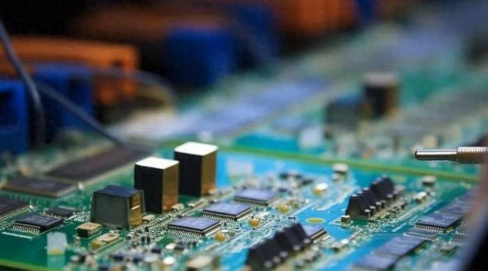
Enhance Low-Cost, Previous-Generation, or Mid-Range SoCs with Caching.
Some design teams, when creating System on Chip (SoC) devices, are fortunate enough to have access to the latest and most advanced technology nodes, and possess a relatively unrestricted budget to obtain Intellectual Property (IP) modules from trusted third-party vendors. However, many engineers are not so fortunate. For every "spare no expense" project, there are a thousand "do the best you can on a limited budget" counterparts.
A method to squeeze maximum performance out of lower-cost, earlier-generation, mid-range processors and accelerator cores is to apply caching wisely.
Cost Reduction
The main technology for interconnecting IPs within an SoC is the Network on Chip (NoC) interconnect IP. This can be viewed as an IP that spans the entire device. The example shown in Figure 1 can be assumed to be a non-cache-coherent scenario. In this case, any coherence requirements would be handled by software.
Assuming the SoC's clock runs at 1GHz. Assuming a Central Processing Unit (CPU) based on a Reduced Instruction Set Computer (RISC) architecture that runs a typical instruction consumes one clock cycle. However, accessing external DRAM memory may require 100 to 200 processor clock cycles (for the purposes of this article, we will average this at 150 cycles). This means that if the CPU has no Level 1 (L1) cache, and is directly connected to DRAM through the NoC and DDR memory controller, then each instruction will consume 150 processor clock cycles, resulting in a CPU utilization rate of only 1/150 = 0.67%.
Advertisement
This is why CPUs, as well as some accelerators and other IPs, use cache memory to improve processor utilization and application performance. The basic principle behind the cache concept is the principle of locality. The idea is that at any given time, only a small part of the main memory is used, and the positions in that space are accessed multiple times. Mainly due to loops, nested loops, and subroutines, instructions and their related data experience temporal, spatial, and sequential locality. This means that once a block of instructions and data is copied from the main memory to the IP's cache, the IP will typically access them repeatedly.
Today's high-end CPU IPs usually have at least a Level 1 (L1) and Level 2 (L2) cache, and they usually also have a Level 3 (L3) cache. In addition, some accelerator IPs, such as Graphics Processing Units (GPUs), usually have their own internal caches. However, the price of these latest-generation high-end IPs is usually 5 to 10 times higher than the previous generation's mid-range products. Therefore, as shown in Figure 1, a cost-conscious SoC's CPU may only be equipped with an L1 cache.Consider the CPU and its L1 cache more deeply. When the CPU requests something from its cache, the outcome is known as a cache hit. Since the L1 cache typically operates at the same speed as the processor core, a cache hit will be processed within a single processor clock cycle. In contrast, if the requested data is not in the cache, the result is called a cache miss, which will require access to main memory, consuming 150 processor clock cycles.
Now consider running 1,000,000 instructions. If the cache is large enough to contain the entire program, then this will only consume 1,000,000 clock cycles, achieving 100% CPU efficiency.
Unfortunately, the L1 cache in a mid-range CPU is typically only 16KB to 64KB in size. If we assume a 95% cache hit rate, then 950,000 of our 1,000,000 instructions will require one processor clock cycle each. The remaining 50,000 instructions will each consume 150 clock cycles. Thus, the CPU efficiency in this scenario can be calculated as 1,000,000 / ((950,000 * 1) + (50,000 * 150)) = ~12%.
Enhancing Performance
A cost-effective way to improve the performance of cost-conscious SoCs is by adding cache IP. For example, Arteris's CodaCache is a configurable, independent non-coherent cache IP. Each CodaCache instance can be up to 8MB, and multiple copies can be instantiated within the same SoC.
The purpose of this article is not to suggest that every IP should be equipped with a CodaCache. Figure 2 is intended only to provide an example of potential CodaCache deployment.
If a CodaCache instance is associated with an IP, it is called a dedicated cache (DC). Alternatively, if a CodaCache instance is associated with a DDR memory controller, it is called a last-level cache (LLC). The DC will accelerate the performance of the IP it is associated with, while the LLC will enhance the performance of the entire SoC.

As an example of the type of performance improvement we might expect, consider the CPU shown in Figure 2. Let's assume that the CodaCache DC instance associated with this IP operates at half the processor speed, and any access to this cache consumes 20 processor clock cycles. If we also assume that this DC has a 95% cache hit rate, then for 1,000,000 instructions—our overall CPU+L1+DC efficiency can be calculated as 1,000,000 / ((950,000 * 1) + (47,500 * 20) + (2,500 * 150)) = ~44%. This is a ~273% performance improvement!
ConclusionIn the past, embedded programmers relished the challenge of squeezing the highest performance possible from small processors with low clock speeds and limited memory resources. In fact, computer magazines often posed challenges to their readers, such as: "Who can execute task X using the fewest clock cycles and the smallest amount of memory on processor Y?"
Today, many SoC developers enjoy the challenge of extracting the highest performance possible from their designs, especially if they are constrained to use mid-range IP with lower performance. Deploying CodaCache IP as a dedicated and last-level cache provides engineers with an affordable way to enhance the performance of their cost-sensitive SoCs.
